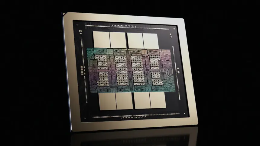
Nvidia has quietly lowered the published memory bandwidth and interconnect specifications for its next-generation Vera Rubin GPUs as production hardware begins reaching cloud providers. The alterations cut per-chip high-bandwidth memory throughput by roughly 13 per cent and reduce NVLink scale-up bandwidth by 17 per cent across rack and server configurations.
Key points
- Nvidia cut the HBM4 memory bandwidth on individual Rubin chips from 22 TB/s to 19.2 TB/s and reduced NVLink 6 speeds from 3.6 TB/s to 3 TB/s.
- The eight-chip HGX Rubin NVL8 server board took the sharpest downgrade, losing 26 per cent of its total memory bandwidth and 300 GB of HBM4 capacity.
- Scale-out networking throughput increased across the lineup by 12.5 per cent, rising to 450 GB/s per GPU.
- The revised figures narrow Nvidia’s lead on paper over AMD’s competing Helios rack systems and Instinct MI455X processors.
Changes to the Rubin silicon
The revised figures appeared without an announcement in documentation updates made during September. Industry watchers at IT Home first identified the alterations by comparing documentation published in October with datasheets released in June 2026. Internet archive records showed the text changed between 1 September and 11 September.
On its official Vera Rubin NVL72 product page, Nvidia now lists each Rubin processor at 19.2 TB/s of HBM4 bandwidth, down from the 22 TB/s listed when the platform was announced. Memory capacity remains at 288 GB per GPU. Theoretical compute performance also stayed level at 50 PFLOPS of sparse NVFP4 inference and 35 PFLOPS of FP4 training.
Interconnect speeds dropped alongside the memory interface. NVLink 6 bandwidth fell from 3.6 TB/s to 3 TB/s per chip. In contrast, scale-out network bandwidth rose from 400 GB/s to 450 GB/s per GPU, providing an unexpected increase for cluster-wide communications across InfiniBand and Ethernet fabrics.

The adjustments mean Nvidia had to pull back on aggressive clock targets for its memory stacks. Standard HBM4 specifications published by JEDEC in April 2025 call for transfer rates of 8 Gbps per pin across a 2,048-bit bus. Reaching 22 TB/s across eight stacks required Nvidia to push memory silicon to approximately 10.75 Gbps per pin. The new 19.2 TB/s figure corresponds to about 9.375 Gbps per pin, which remains above standard industry rates but lowers operational demands on memory controllers.
Rack-scale adjustments for NVL72
The reductions on individual chips translate directly into smaller totals at the cluster level. In the flagship Vera Rubin NVL72 rack, which joins 72 Rubin GPUs with 36 Vera CPUs and BlueField-4 data processing units, total memory bandwidth fell from 1,580 TB/s to 1,400 TB/s. Total memory capacity held firm at 20.7 TB.
Aggregate NVLink fabric bandwidth across the NVL72 dropped from 260 TB/s to 216 TB/s. Meanwhile, total scale-out networking bandwidth climbed from 28.8 TB/s to 32.4 TB/s bidirectional, reflecting the networking boost applied to each GPU tray. The dual-chip Vera Rubin Superchip module dropped from 44 TB/s of aggregate memory bandwidth to 38.5 TB/s.
Nvidia has left its efficiency claims intact on promotional pages, still advertising up to ten times more tokens per megawatt than Blackwell GB200 systems. However, those claims carry footnotes stating figures remain subject to change, and the company has not confirmed whether its performance models were recalculated using the 19.2 TB/s baseline.

Severe cuts on HGX server boards
While the NVL72 rack saw proportional cuts, the standard eight-way board designed for traditional enterprise data centres sustained deeper losses. Specifications on the official HGX page show aggregate memory capacity dropping from 2.3 TB to 2 TB across the board, alongside an aggregate bandwidth fall from 176 TB/s to 130 TB/s.
That represents a 26 per cent reduction in memory throughput. Dense training compute on the HGX board fell from 280 to 270 PFLOPS for NVFP4, and from 140 to 130 PFLOPS for FP8 formats. NVLink Switch bandwidth dropped from 28.8 TB/s to 24 TB/s.
The 2 TB system capacity indicates that individual GPUs on the HGX board provide roughly 250 GB of memory rather than the full 288 GB. Disabling one of the eight physical HBM4 stacks on each processor would account for both the lower capacity and the 16.25 TB/s per-GPU bandwidth total. Nvidia previously disabled memory stacks to improve manufacturing yields on early versions of its H100 accelerator.
Memory supply pressures
Engineering compromises around HBM4 have loomed over the Rubin generation for more than a year. TrendForce reported in September 2025 that Nvidia was urging memory suppliers to hit 10 Gbps pin speeds to counter rival architectures, warning that yield shortages could force the company to abandon speed upgrades or segment product lines.
By early 2026, memory makers faced requests exceeding 11 Gbps. Although Samsung and SK hynix managed early sample runs at elevated frequencies, maintaining acceptable yields at commercial volumes proved difficult. Reining in clock rates allows Nvidia to secure reliable volumes from its packaging partners without holding up autumn deliveries.
Jensen Huang, Nvidia’s chief executive, told investors in August that Vera Rubin was in full production to support cloud deployments. Adjusting the specifications down ensures systems can clear factory validation at scale rather than stalling on silicon binning.
How does Rubin compare with AMD Helios?
The revised specifications alter the paper contest between Nvidia and AMD in the top tier of data centre silicon. AMD designed its Instinct MI455X accelerator with 12 HBM4 stacks running across a wider bus at 7.6 Gbps per pin, below the JEDEC ceiling. That design yields 23.3 TB/s of memory bandwidth and 432 GB of capacity per GPU without demanding pushed memory clocks.
When AMD launched its Helios rack system, it claimed a slight lead in memory throughput over Nvidia’s preliminary targets. Against the revised 1,400 TB/s specification of the NVL72, Helios holds a paper advantage of roughly 19 per cent in total memory bandwidth. AMD also holds a paper lead in scale-up fabric throughput, though benchmark comparisons under realistic model workloads have not yet been published.
Raw memory bandwidth serves as a critical constraint for large language model inference, where memory buses dictate how quickly weights transfer during token generation. Even with the cuts, Rubin provides about 2.4 times the per-chip memory bandwidth of the Blackwell generation, which offered 8 TB/s.
Major cloud providers are already putting the hardware into service, with Oracle opening commercial access to early NVL72 clusters. Enterprise customers and server integrators are scheduled to receive production shipments of the HGX Rubin boards through the end of 2026.