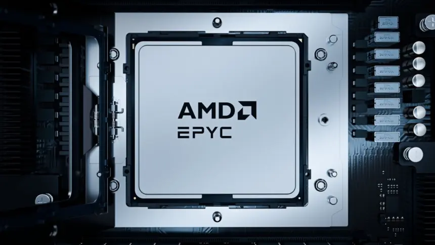
AMD launched its AMD EPYC Venice server processor family on 10 November 2026, introducing the Zen 6 microarchitecture to enterprise data centres. The EPYC 9006 series scales up to 256 cores per socket and targets demanding agentic AI and cloud computing workloads with faster memory links and PCIe 6.0 connectivity.
Zen 6 microarchitecture and compute density
The launch marks the debut of AMD’s Zen 6 core architecture, manufactured on TSMC’s 2-nanometre N2P process for the compute dies. AMD pairs these with two input-output dies fabricated on TSMC’s 3-nanometre node, changing the single-hub layout used in earlier generations.
AMD is releasing two core variants: the standard Zen 6 core and the denser Zen 6c core. A single Zen 6 core complex die holds up to 12 cores with 48 megabytes of shared L3 cache, compared to eight cores in Zen 5. The Zen 6c complex doubles previous density, fitting 32 cores and 128 megabytes of L3 cache onto each die.
Across enterprise, cloud and AI workloads, AMD claims an average 27 per cent instructions-per-clock uplift over Zen 5, according to Wccftech. In AI-specific operations, that instructions-per-clock gain reaches 31 per cent.
Inside the execution engine, AMD split the integer schedulers into 96 shared and 48 dedicated units. The vector engine now natively processes 16-bit floating-point math within its 512-bit data path, eliminating conversion steps required by Zen 5, and doubles the 8-bit vector neural network execution pipelines from two to four.
Memory channels, PCIe 6.0 and early benchmarks
The initial Venice rollout uses AMD’s new SP7 socket, measuring 76 by 80 millimetres. The dual input-output dies provide 16 memory channels per socket, supporting second-generation MRDIMMs at up to 12,800 megatransfers per second. That gives each socket up to 1.6 terabytes per second of memory bandwidth and up to 8 terabytes of system memory.

For connectivity, single-socket SP7 systems offer 96 PCIe 6.0 lanes, while dual-socket servers supply up to 128 lanes running at 64 gigabits per second per lane, alongside CXL 3.1 support. Power limits for SP7 processors reach up to 600 watts.
Independent testing by Tom’s Hardware examined a dual-socket server running two flagship EPYC 9996 processors. The 512-core, 1,024-thread configuration produced a 93 per cent throughput increase over previous-generation Turin hardware in SPEC CPU integer tests.
AMD also adjusted clock frequencies for its frequency-focused EPYC 9686F processor ahead of the launch. The 96-core chip now clocks up to 5.3 GHz rather than the 5.0 GHz figure AMD announced earlier, as reported by ServeTheHome. AMD told reviewers that final silicon yielded better than expected, allowing the chip to compete against Nvidia’s Vera processor in high-performance computing.
Software memory expansion and rack power control
Alongside the hardware revisions, AMD introduced MEXT, a software tier that treats flash storage as system memory. Acquired earlier this year, MEXT uses a transformer model inside a Linux kernel module to predict which memory pages an application will need next and streams them from solid-state storage before latency penalties occur.
AMD internal testing across 145 servers running chip-design software showed systems kept 95 per cent of their application performance while using half the physical DRAM. Hewlett Packard Enterprise will offer hardware configurations prepared for the software, and AMD plans to expand its internal deployment to more than 2,000 servers next year.
To manage data centre energy budgets, Venice introduces three power control systems: Unified Power Provisioning, Utilization-Based Power Scaling, and Frequency-Adaptive Spectrum Technology, known as FAST. AMD described the feature as enabling “multiple commercial SKUs within a single socket”—allowing operators to allocate some cores to high-frequency priority tasks while keeping other cores at lower power for batch processing.
These power management features reflect a broader industry push to make server hardware operate efficiently inside existing electrical limits, complementing other infrastructure trials such as rack-scale AI testing designed to curb system power consumption.
What comes next for Venice?
AMD plans to widen the EPYC 9006 family early next year by releasing the SP8 socket. The smaller 62.5 by 80 millimetre design scales up to 128 cores with eight memory channels and up to 192 PCIe 6.0 lanes, capped at 400 watts.
Further extensions include Venice-X chips equipped with 3D V-Cache for simulation workloads, and the Verano superchip family. Verano will combine Zen 6 cores with low-power double data rate memory to compete against combined CPU and GPU platforms, according to The Register.
AMD held a 46 per cent revenue share of the x86 server processor market entering the Venice launch. The company projected that its data centre revenue would surpass Intel‘s in the fourth quarter of 2026.