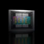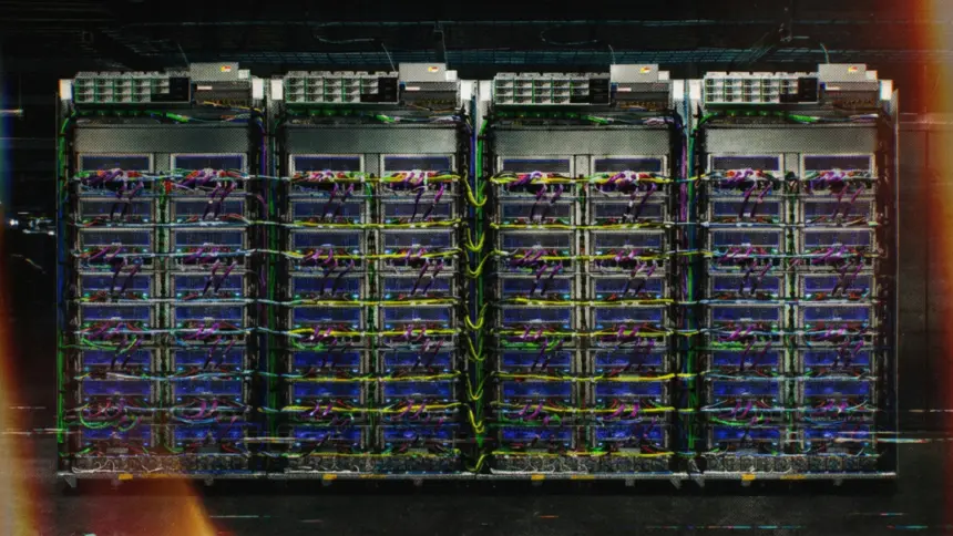
Google introduced two new hardware systems on Monday to expand its eighth-generation accelerator family, adding specialised Google TPU chips engineered for confidential computing and context scaling. The TPU 8tx and TPU 8i Max adapt existing processor silicon into dense server configurations for enterprises and government agencies running complex artificial intelligence models.
The announcement means Google has delivered four tensor processing unit systems within a single calendar year for the first time, as The Decoder reported. At its Google Cloud Next conference in April, the company introduced the first two entries in the generation: the TPU 8t for large-scale training and the TPU 8i for real-time inference.
According to Data Center Dynamics, Google designed the TPU 8tx specifically for confidential computing and the TPU 8i Max for context scaling. Neither system uses newly fabricated silicon. Google instead combined existing processors with altered packaging, memory layouts, and networking connections.
Amin Vahdat, Google’s chief technologist for AI infrastructure, told Bloomberg News that the variants are reconfigured systems designed to handle workloads customers have requested. The modular architecture allows Google to assemble and deliver hardware variants within months rather than waiting years for new chip designs.
Alphabet shares rose more than 2% in premarket trading following the news, The Economic Times reported. Alphabet shares had dropped 9% this year through Friday’s close. Reuters reported that Alphabet did not immediately respond to a request for comment.
What is the TPU 8tx and how does it protect data?
The TPU 8tx targets government agencies and enterprises operating in regulated industries that must protect sensitive records. Organisations routinely encrypt data while it rests in storage or travels across networks, but standard hardware requires that information to be decrypted in system memory before a processor can compute calculations on it.

Google addressed that security gap by building a secure enclave directly into the hardware layer, SiliconANGLE reported. The design ensures data and model weights remain isolated and protected during active calculations. Nvidia offers a comparable security feature on its graphics processing units through its confidential computing architecture.
Built on the same physical architecture as the TPU 8t, the 8tx runs alongside custom AMD host central processing units. It connects over Google’s proprietary Boardfly network, which was originally developed for real-time inference and offers up to twice the latency reduction of the standard TPU 8t.
The system combines training-level computational power with fast inference. That combination allows regulated organisations to fine-tune models on private data, distil large models into smaller ones, and train autonomous agents using reinforcement learning on a single setup, eliminating the need to transfer unencrypted data between different server clusters.
How the TPU 8i Max handles context scaling
The second system, the TPU 8i Max, is designed to resolve memory constraints that occur when artificial intelligence models evaluate large collections of data. Tasks such as inspecting long software codebases, hours of video, or extended conversation histories demand extensive context windows, which represent the volume of information an AI model can hold in working memory while formulating answers.
Expanding the context window strains hardware because processors must repeatedly swap information in and out of memory. To alleviate that bottleneck, Google combined two TPU 8i chips onto a single physical package.
Mounting two chips on one package doubles the compute performance, static random-access memory, and high-bandwidth memory compared to the standard TPU 8i. The configuration also doubles memory bandwidth within the same rack structure.
Because the design fits twice as much silicon into the same physical rack footprint, it reduces the data centre floor space required per square foot and per watt. Increasing on-chip memory limits the need to move data between separate processors, which lowers operating latency and cuts the electrical power an AI model consumes while processing queries.
Google developed the TPU 8i Max alongside its work on its Gemini frontier models, which support context windows of 1 million tokens, representing roughly 750,000 words or 1,500 pages of text. While flagship models process 1 million tokens, smaller models often support narrower windows between 128,000 and 256,000 tokens.
Software tools for cloud customers
To help external software teams use the hardware, Google released TorchTPU as an open-source tool. The software allows developers to run standard PyTorch code on TPU hardware with minimal code alterations.
Google has also integrated support for popular open-source inference frameworks, including vLLM and SGLang. These software additions support Google’s shift from keeping custom silicon for internal services to selling accelerator access directly to commercial cloud clients.
Google now counts nearly 100 external customers using its TPU cloud infrastructure. Homegrown accelerators, once reserved solely for internal use, have become an external commercial offering.
How do Google’s TPU chips challenge Nvidia?
The broader technology sector is experiencing a spending pivot, as companies direct more capital toward running live models rather than funding expensive initial training runs. Specialised accelerators offer distinct operational efficiencies for day-to-day inference workloads.
That shift has led other major technology firms to design custom accelerators to curb reliance on Nvidia‘s expensive graphics processors. Amazon, Microsoft, and OpenAI are all pursuing internal chip projects.
Nvidia has acted to defend its lead in the AI infrastructure market. The company recently completed an acqui-hire and licensing agreement with Groq to bolster its own inference capabilities as competition over custom accelerators intensifies.